The macroscopic demonstrations described above, repeating Newton’s original tests on the adhesion of glass lenses, give an insight into the laws of adhesion. Newton had seen two of the three indicators of molecular adhesion: the black, flattened contact spot, and the pull-off force. But he had not seen the spontaneous jumping into contact. The reason was that, with large hard spheres, the adhesion could not be established reproducibly because surface roughness and dust particles prevented true molecular contact. Rubber spheres get over that problem to a certain extent because they are softer. The other approach is to make the spheres smaller and smaller. For small particles, roughness is less of a problem and adhesion is then always observable, even between the hardest surfaces. As particles are made very small, they begin to approach the size of single molecules, or ultimately single atoms, which always adhere.
It would be a superb experiment if two molecules could be gripped, brought together, and then pulled apart to measure their molecular adhesion. Unfortunately no-one has yet found a way to do this (see Chapter 13). And the very act of gripping the molecules would change their character by preventing Brownian motion, and also distorting their electronic attractive fields of influence.
A much more practical experiment became possible with the invention of the atomic force microscope by Binnig, Quate and Gerber14 in 1986. This device
|
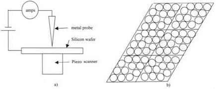
Figure 3.16. (a) Binnig and Rohrer’s experiment on electron conduction through a fine contact, (b) The surface structure of silicon revealed by scanning the sample under the probe, showing the adatoms sitting on the 7 x 7 unit cell of the (111) surface. |
followed from Binnig and Rohrer’s work at IBM on the contact between a fine metal probe and a very flat surface, such as a silicon wafer used in electronic chips. Binnig, Rohrer and colleagues15 were working in the tradition of Ragnar Holm on the electrical conduction through metal contacts. Holm had seen that only a small part of an electrical contact actually conducts electrons, and concluded that the true molecular contact was small. Binnig and co-workers used finer and finer metal probes to show that the ultimate contact between a wire and a surface was a single atom. When the sample was moved beneath the tip, using a piezoelectric scanner, it received electrons from each atom in turn and produced an atomic picture of the surface, as shown in Fig. 3.16.
This was the first time that the strange diamond patterned arrangement of adatoms on the surface of a silicon wafer had been seen directly, although it had been suspected from previous spectroscopic measurements of silicon surfaces. For this remarkable instrument, now called the scanning tunneling microscope, Binnig and Rohrer received the Nobel Prize in 1986.
 12 сентября, 2015
  Pokraskin
 Опубликовано в рубрике